


 Add to like
 Add to project list
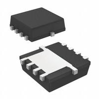 123
123
- Home >
- Manufacturer No:
- Manufacturer:
- Category:
- Datasheet:
- SKU:
- Description:
- Quantity:
- RFQ
Add To Cart
- Material flow:


- Payment:


Inventory:9837
- Qty Unit Price price
- 1 $1.011 $1.011
- 10 $1 $10
- 100 $0.99 $99
- 1000 $0.98 $980
- 10000 $0.97 $9700
Not the price you want? Send RFQ Now and we'll contact you ASAP
- Manufacturer No:SI7119DN-T1-E3
- Manufacturer:Vishay Siliconix
- Category:Transistors - FETs, MOSFETs - Single
- Datasheet:SI7119DN-T1-E3
- SKU:276278
- Description:MOSFET P-CH 200V 3.8A 1212-8


User Guide


User Guide

SI7119DN-T1-E3 Details
MOSFET P-CH 200V 3.8A 1212-8

SI7119DN-T1-E3 Specification Parameters
- Part Status: Active
- Moisture Sensitivity Level (MSL): 1 (Unlimited)
- Mount: Surface Mount
- Number of Elements: 1
- ECCN Code: EAR99
- Radiation Hardening: No
- Lead Free: Lead Free
- Pin Count: 8
- Published: 2013
- Number of Terminations: 5
- Terminal Finish: Matte Tin (Sn)
- Factory Lead Time: 14 Weeks
- Transistor Element Material: SILICON
- Gate to Source Voltage (Vgs): 20V
- Transistor Application: SWITCHING
- Vgs (Max): ±20V
- Subcategory: Other Transistors
- Length: 3.05mm
- FET Type: P-Channel
- Fall Time (Typ): 12 ns
- Series: TrenchFET?
- Drive Voltage (Max Rds On,Min Rds On): 6V 10V
- Rise Time: 11ns
- Gate Charge (Qg) (Max) @ Vgs: 25nC @ 10V
- Operating Temperature: -50°C~150°C TJ
- Drain to Source Breakdown Voltage: -200V
- Power Dissipation-Max: 3.7W Ta 52W Tc
- Continuous Drain Current (ID): -3.8A
- Input Capacitance (Ciss) (Max) @ Vds: 666pF @ 50V
- RoHS Status: ROHS3 Compliant
- Mounting Type: Surface Mount
- Packaging: Tape & Reel (TR)
- Number of Channels: 1
- Pbfree Code: yes
- JESD-609 Code: e3
- Number of Pins: 8
- Terminal Position: DUAL
- Peak Reflow Temperature (Cel): 260
- Drain to Source Voltage (Vdss): 200V
- Time@Peak Reflow Temperature-Max (s): 40
- Pulsed Drain Current-Max (IDM): 5A
- Element Configuration: Single
- Technology: MOSFET (Metal Oxide)
- Operating Mode: ENHANCEMENT MODE
- Terminal Form: C BEND
- Case Connection: DRAIN
- Width: 3.05mm
- Vgs(th) (Max) @ Id: 4V @ 250μA
- Turn On Delay Time: 9 ns
- Turn-Off Delay Time: 27 ns
- Height: 1.04mm
- Resistance: 1.05Ohm
- Power Dissipation: 3.7W
- Package / Case: PowerPAK? 1212-8
- JESD-30 Code: S-XDSO-C5
- Current - Continuous Drain (Id) @ 25°C: 3.8A Tc
- Rds On (Max) @ Id, Vgs: 1.05 Ω @ 1A, 10V
Search for similar products

SI7119DN-T1-E3 Similar Products
The four parts on the right have similar specifications to Vishay Siliconix & SI7119DN-T1-E3


Hot Search
Excellent
Based on reviews
Excellent
Based on reviews
LKR uses cookies to help deliver a better online experience. You can see what cookies we server and how to set your preferences in our
Cookies Policy, if you agree on our use of cookies please click continue. When browsing and using our website, LKR also collects, stores and/or processes personal data,
please read our Term & Condition
and
Privacy Policy
to find out more.

About Us


Our social media


We support logistics


We Accept Payment Via